- 您现在的位置:买卖IC网 > Sheet目录3873 > PIC16CR76T-I/SS (Microchip Technology)IC PIC MCU 8KX14 28SSOP
PIC18F2220/2320/4220/4320
DS39599G-page 112
2007 Microchip Technology Inc.
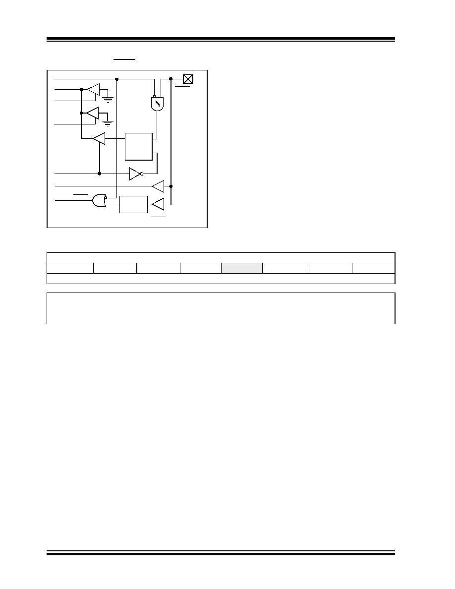
FIGURE 10-14:
BLOCK DIAGRAM OF
MCLR/VPP/RE3 PIN
MCLR/VPP/
Data Bus
RD PORTE
RD LATE
Schmitt
Trigger
MCLRE
RD TRISE
QD
EN
Latch
Filter
Low-Level
MCLR Detect
High-Voltage Detect
Internal MCLR
HV
RE3
REGISTER 10-1:
TRISE REGISTER
R-0
R/W-0
U-0
R/W-1
IBF
OBF
IBOV
PSPMODE
—
TRISE2
TRISE1
TRISE0
bit 7
bit 0
Legend:
R = Readable bit
W = Writable bit
U = Unimplemented bit, read as ‘0’
-n = Value at POR
‘1’ = Bit is set
‘0’ = Bit is cleared
x = Bit is unknown
bit 7
IBF: Input Buffer Full Status bit
1 = A word has been received and waiting to be read by the CPU
0 = No word has been received
bit 6
OBF: Output Buffer Full Status bit
1 = The output buffer still holds a previously written word
0 = The output buffer has been read
bit 5
IBOV: Input Buffer Overflow Detect bit (in Microprocessor mode)
1 = A write occurred when a previously input word has not been read (must be cleared in software)
0 = No overflow occurred
bit 4
PSPMODE: Parallel Slave Port Mode Select bit
1 = Parallel Slave Port mode
0 = General Purpose I/O mode
bit 3
Unimplemented: Read as ‘0’
bit 2
TRISE2: RE2 Direction Control bit
1 = Input
0 = Output
bit 1
TRISE1: RE1 Direction Control bit
1 = Input
0 = Output
bit 0
TRISE0: RE0 Direction Control bit
1 = Input
0 = Output
发布紧急采购,3分钟左右您将得到回复。
相关PDF资料
PIC18F13K50-I/P
IC PIC MCU FLASH 4KX16 20-PDIP
PIC16CR76T-I/SO
IC PIC MCU 8KX14 28SOIC
PIC18LF24K22-I/MV
IC PIC MCU 16KB FLASH 28UQFN
PIC18LF24K22-I/ML
IC PIC MCU 16KB FLASH 28QFN
PIC16CR76T-I/ML
IC PIC MCU 8KX14 28QFN
PIC16F627-04/P
IC MCU FLASH 1KX14 COMP 18DIP
PIC18F45J10-I/ML
IC PIC MCU FLASH 16KX16 44QFN
PIC18F24K22-I/ML
IC PIC MCU 16KB FLASH 28QFN
相关代理商/技术参数
PIC16CR77-I/ML
功能描述:IC PIC MCU 8KX14 44QFN RoHS:是 类别:集成电路 (IC) >> 嵌入式 - 微控制器, 系列:PIC® 16C 产品培训模块:Asynchronous Stimulus
8-bit PIC® Microcontroller Portfolio 标准包装:42 系列:PIC® 16C 核心处理器:PIC 芯体尺寸:8-位 速度:20MHz 连通性:- 外围设备:欠压检测/复位,POR,PWM,WDT 输入/输出数:13 程序存储器容量:3.5KB(2K x 14) 程序存储器类型:OTP EEPROM 大小:- RAM 容量:128 x 8 电压 - 电源 (Vcc/Vdd):4 V ~ 5.5 V 数据转换器:A/D 4x8b 振荡器型:外部 工作温度:-40°C ~ 85°C 封装/外壳:18-SOIC(0.295",7.50mm 宽) 包装:管件 配用:XLT18SO-1-ND - SOCKET TRANSITION 18SOIC 300MILISPICR1-ND - ADAPTER IN-CIRCUIT PROGRAMMING309-1011-ND - ADAPTER 18-SOIC TO 18-DIP309-1010-ND - ADAPTER 18-SOIC TO 18-DIPAC164010-ND - MODULE SKT PROMATEII DIP/SOIC
PIC16CR77-I/P
功能描述:IC PIC MCU 8KX14 40DIP RoHS:是 类别:集成电路 (IC) >> 嵌入式 - 微控制器, 系列:PIC® 16C 产品培训模块:Asynchronous Stimulus
8-bit PIC® Microcontroller Portfolio 标准包装:42 系列:PIC® 16C 核心处理器:PIC 芯体尺寸:8-位 速度:20MHz 连通性:- 外围设备:欠压检测/复位,POR,PWM,WDT 输入/输出数:13 程序存储器容量:3.5KB(2K x 14) 程序存储器类型:OTP EEPROM 大小:- RAM 容量:128 x 8 电压 - 电源 (Vcc/Vdd):4 V ~ 5.5 V 数据转换器:A/D 4x8b 振荡器型:外部 工作温度:-40°C ~ 85°C 封装/外壳:18-SOIC(0.295",7.50mm 宽) 包装:管件 配用:XLT18SO-1-ND - SOCKET TRANSITION 18SOIC 300MILISPICR1-ND - ADAPTER IN-CIRCUIT PROGRAMMING309-1011-ND - ADAPTER 18-SOIC TO 18-DIP309-1010-ND - ADAPTER 18-SOIC TO 18-DIPAC164010-ND - MODULE SKT PROMATEII DIP/SOIC
PIC16CR77-I/PT
功能描述:IC PIC MCU 8KX14 44TQFP RoHS:是 类别:集成电路 (IC) >> 嵌入式 - 微控制器, 系列:PIC® 16C 产品培训模块:Asynchronous Stimulus
8-bit PIC® Microcontroller Portfolio 标准包装:42 系列:PIC® 16C 核心处理器:PIC 芯体尺寸:8-位 速度:20MHz 连通性:- 外围设备:欠压检测/复位,POR,PWM,WDT 输入/输出数:13 程序存储器容量:3.5KB(2K x 14) 程序存储器类型:OTP EEPROM 大小:- RAM 容量:128 x 8 电压 - 电源 (Vcc/Vdd):4 V ~ 5.5 V 数据转换器:A/D 4x8b 振荡器型:外部 工作温度:-40°C ~ 85°C 封装/外壳:18-SOIC(0.295",7.50mm 宽) 包装:管件 配用:XLT18SO-1-ND - SOCKET TRANSITION 18SOIC 300MILISPICR1-ND - ADAPTER IN-CIRCUIT PROGRAMMING309-1011-ND - ADAPTER 18-SOIC TO 18-DIP309-1010-ND - ADAPTER 18-SOIC TO 18-DIPAC164010-ND - MODULE SKT PROMATEII DIP/SOIC
PIC16CR77T-I/ML
功能描述:IC PIC MCU 8KX14 44QFN RoHS:是 类别:集成电路 (IC) >> 嵌入式 - 微控制器, 系列:PIC® 16C 产品培训模块:Asynchronous Stimulus
8-bit PIC® Microcontroller Portfolio 标准包装:42 系列:PIC® 16C 核心处理器:PIC 芯体尺寸:8-位 速度:20MHz 连通性:- 外围设备:欠压检测/复位,POR,PWM,WDT 输入/输出数:13 程序存储器容量:3.5KB(2K x 14) 程序存储器类型:OTP EEPROM 大小:- RAM 容量:128 x 8 电压 - 电源 (Vcc/Vdd):4 V ~ 5.5 V 数据转换器:A/D 4x8b 振荡器型:外部 工作温度:-40°C ~ 85°C 封装/外壳:18-SOIC(0.295",7.50mm 宽) 包装:管件 配用:XLT18SO-1-ND - SOCKET TRANSITION 18SOIC 300MILISPICR1-ND - ADAPTER IN-CIRCUIT PROGRAMMING309-1011-ND - ADAPTER 18-SOIC TO 18-DIP309-1010-ND - ADAPTER 18-SOIC TO 18-DIPAC164010-ND - MODULE SKT PROMATEII DIP/SOIC
PIC16CR77T-I/PT
功能描述:IC PIC MCU 8KX14 44TQFP RoHS:是 类别:集成电路 (IC) >> 嵌入式 - 微控制器, 系列:PIC® 16C 产品培训模块:Asynchronous Stimulus
8-bit PIC® Microcontroller Portfolio 标准包装:42 系列:PIC® 16C 核心处理器:PIC 芯体尺寸:8-位 速度:20MHz 连通性:- 外围设备:欠压检测/复位,POR,PWM,WDT 输入/输出数:13 程序存储器容量:3.5KB(2K x 14) 程序存储器类型:OTP EEPROM 大小:- RAM 容量:128 x 8 电压 - 电源 (Vcc/Vdd):4 V ~ 5.5 V 数据转换器:A/D 4x8b 振荡器型:外部 工作温度:-40°C ~ 85°C 封装/外壳:18-SOIC(0.295",7.50mm 宽) 包装:管件 配用:XLT18SO-1-ND - SOCKET TRANSITION 18SOIC 300MILISPICR1-ND - ADAPTER IN-CIRCUIT PROGRAMMING309-1011-ND - ADAPTER 18-SOIC TO 18-DIP309-1010-ND - ADAPTER 18-SOIC TO 18-DIPAC164010-ND - MODULE SKT PROMATEII DIP/SOIC
PIC16CR83T-04/SO023
制造商:Microchip Technology Inc 功能描述:
PIC16F
制造商:Microchip Technology Inc 功能描述:Microchip PIC16F677-I/P Microcontroller
PIC16F1454-E/ML
制造商:Microchip Technology Inc 功能描述:7 KB FLASH, 512 BYTES RAM, 48 MHZ INT. OSC, 12 I/0, ENHANCED - Rail/Tube 制造商:Microchip Technology Inc 功能描述:IC MCU 8BIT 7KB FLASH 16QFN